- 您现在的位置:买卖IC网 > Sheet目录350 > PCA9685PW,118 (NXP Semiconductors)IC LED DRIVER RGBA 28-TSSOP
NXP Semiconductors
PCA9685
16-channel, 12-bit PWM Fm+ I 2 C-bus LED controller
SDA
t BUF
t r
t f
t HD;STA
t SP
t LOW
SCL
t HD;STA
t SU;STA
t SU;STO
P
S
t HD;DAT
t HIGH
t SU;DAT
Sr
P
002aaa986
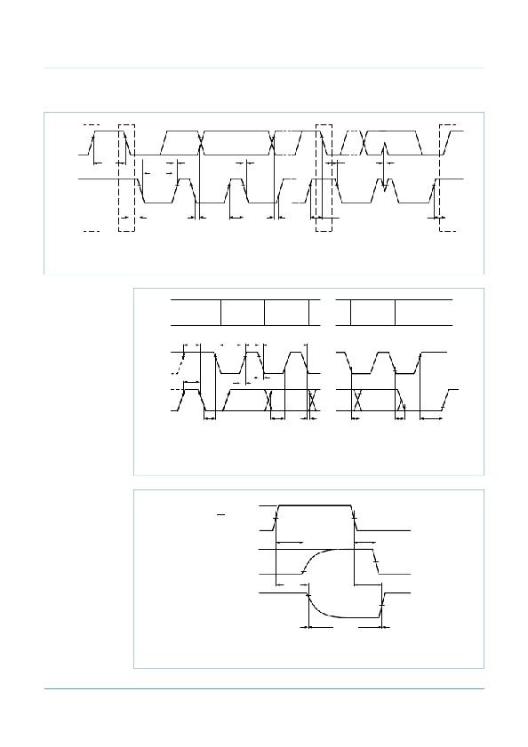
Fig 31. Definition of timing
protocol
START
condition
(S)
bit 7
MSB
(A7)
bit 6
(A6)
bit 1
(D1)
bit 0
(D0)
acknowledge
(A)
STOP
condition
(P)
t SU;STA
t LOW
t H IG H
1 / f SCL
SCL
SDA
t BUF
t r
t f
t HD;STA
t SU;DAT
t HD;DAT
t VD;DAT
t VD;ACK
t SU;STO
002aab285
Rise and fall times refer to V IL and V IH .
Fig 32. I 2 C-bus timing diagram
V I
OE input
V SS
V M
t PLZ
V M
t PZL
LEDn output
LOW-to-OFF
V DD
V M
OFF-to-LOW
LEDn output
V OL
V OH
t PHZ
V X
V Y
t PZH
HIGH-to-OFF
V M
OFF-to-HIGH
V SS
outputs
enabled
outputs
disabled
outputs
enabled
002aad810
Fig 33. t PLZ , t PZL and t PHZ , t PZH times
PCA9685
Product data sheet
All information provided in this document is subject to legal disclaimers.
Rev. 3 — 2 September 2010
? NXP B.V. 2010. All rights reserved.
41 of 51
发布紧急采购,3分钟左右您将得到回复。
相关PDF资料
PCA9922PW,118
IC LED DRIVER LINEAR 16-TSSOP
PCA9955TW,118
IC LED DRVR CONST CURR
PCF85102C-2P/03,11
IC EEPROM 2KBIT 100KHZ 8DIP
PCF85103C-2T/00,11
IC EEPROM 2KBIT 100KHZ 8SOIC
PCF8570T/F5,512
IC SRAM 2KBIT 100KHZ 8SOIC
PCF8582C-2T/03,118
IC EEPROM 2KBIT 100KHZ 8SOIC
PCF8594C-2T/02,118
IC EEPROM 4KBIT 100KHZ 8SOIC
PCF8598C-2P/02,112
IC EEPROM 8KBIT 100KHZ 8DIP
相关代理商/技术参数
PCA9685PW/Q900,118
功能描述:LED显示驱动器 LED Driver 2.3V-5.5V 6mA RoHS:否 制造商:Micrel 数位数量:5 片段数量: 安装风格:SMD/SMT 封装 / 箱体:PLCC-44 工作电源电压:4.75 V to 11 V 最大电源电流:10 mA 最大工作温度:+ 85 C 最小工作温度:- 40 C 封装:Tube
PCA9691BS/1
制造商:NXP Semiconductors 功能描述:IC ADC/DAC 8-BIT I2C 16-HVQFN 制造商:NXP Semiconductors 功能描述:IC, ADC/DAC, 8-BIT, I2C, 16-HVQFN
PCA9691BS/1,118
功能描述:I2C 接口集成电路 ADC/DAC 16-Pin HVQFN EP RoHS:否 制造商:NXP Semiconductors 电源电压-最大:5.5 V 电源电压-最小:2.3 V 最大工作频率:400 KHz 最大工作温度:+ 85 C 封装 / 箱体:TSSOP-16
PCA9691BS/1118
制造商:NXP Semiconductors 功能描述:PCA9691BS/HVQFN16/REEL13//1
PCA9691T/1,112
制造商:NXP Semiconductors 功能描述:
PCA9691T/1,118
制造商:NXP Semiconductors 功能描述:
PCA9691T/1,512
功能描述:I2C 接口集成电路 8b A/D AND D/A COVERTER RoHS:否 制造商:NXP Semiconductors 电源电压-最大:5.5 V 电源电压-最小:2.3 V 最大工作频率:400 KHz 最大工作温度:+ 85 C 封装 / 箱体:TSSOP-16
PCA9691T/1,518
功能描述:模数转换器 - ADC 8-bit A/D and D/A converter RoHS:否 制造商:Texas Instruments 通道数量:2 结构:Sigma-Delta 转换速率:125 SPs to 8 KSPs 分辨率:24 bit 输入类型:Differential 信噪比:107 dB 接口类型:SPI 工作电源电压:1.7 V to 3.6 V, 2.7 V to 5.25 V 最大工作温度:+ 85 C 安装风格:SMD/SMT 封装 / 箱体:VQFN-32
